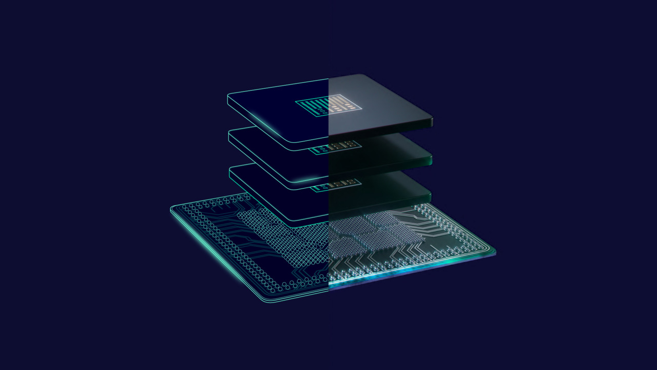
Advanced packaging combines separate pieces of silicon—such as processors and memory—into a single unit. Unlike traditional packaging, which mainly protects components and connects them to circuit boards, these techniques help chips exchange data more quickly, a key factor in training and running AI models.
Some graphics and central processing units now contain more than 10 individual chips, and some designs include as many as 20. Pat Gelsinger, former Intel chief executive and now a partner at Playground Global, estimates advanced packaging could eventually account for as much as half the value of a chip product. Research firm Yole Group forecasts that advanced-packaging revenue will surpass traditional packaging revenue for the first time in 2026; capital spending is expected to approach $28 billion.
TSMC leads in sophisticated packaging, including its chip-on-wafer-on-substrate (CoWoS) process, used by Nvidia, AMD and Broadcom, as well as cloud companies developing their own AI processors. Capacity constraints are pushing customers to seek other suppliers. Nvidia is reportedly providing billions of dollars to expand CoWoS capacity at Siliconware Precision Industries (SPIL), an ASE Technology subsidiary. An industry executive familiar with the arrangement said the financing will support factory space and equipment.
Taiwanese firms are also developing alternatives. Powertech Technology (PTI) is working with AMD and Broadcom on panel-level packaging, which uses larger rectangular panels instead of round wafers and could fit more chips into each production cycle with less material waste. PTI chairman D.K. Tsai said the company plans to invest $400 million in an advanced-packaging joint venture with Broadcom in Singapore, with production potentially starting in 2028.
TSMC has its own panel-based technology, chip-on-panel-on-substrate (CoPoS). It said in April that a pilot line was established and manufacturing was expected to begin within a couple of years; CoWoS remains its main packaging technology for AI chips. AMD has announced more than $10 billion in investments across Taiwan’s semiconductor sector, including partnerships with ASE, SPIL and Powertech. Chief executive Lisa Su has called for more packaging capacity while describing TSMC as an important partner. Microsoft Azure hardware chief Rani Borkar has cited potential material savings from panel-level packaging, but Microsoft has not decided whether or when to adopt it.
Equipment suppliers Tokyo Electron and Applied Materials are targeting the expanding market. Tokyo Electron Taiwan president Seiji Nakama has pointed to advanced packaging’s faster growth compared with the broader semiconductor equipment market. An Applied Materials executive expects the market, including panel-level packaging, to grow substantially over the next three to five years.
The expansion of alternatives could ease reliance on a limited number of facilities, but panel-level packaging’s commercial prospects depend on proving it can deliver reliable production at the scale and complexity leading chip designers need. Information from Reuters.



Comments (0)
No comments yet. Be the first!